Graphene and boron nitride can form semiconductor
Post Date: 03 Dec 2013 Viewed: 361
Menno Bokdam, a PhD student from the University of Twente's Institute for Nanotechnology, has examined the interaction between graphene and boron nitride and proposes the two materials could be used to create semiconductors.

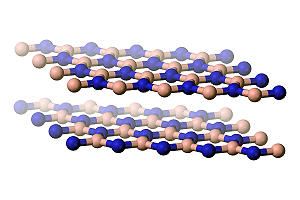
Both materials are thin and have almost the same 'chicken wire' structures. However, boron nitride does not conduct electricity. When placed on top of one another, a redistribution of electrons in the graphene can be seen, creating electrons and 'holes'. Bokdam contends that, if the angle between the two mesh structures is chosen precisely, a 'gap' is also revealed between occupied and unoccupied energy states. He says an electron must overcome this gulf in order to conduct electricity and notes this is a defining characteristic for a semiconductor.
When this combination of graphene and boron nitride is applied on a copper substrate, a charge distribution, or dipole layer, is formed at the interface between copper and boron nitride. This charge can tunnel through the boron nitride, although it does not conduct electricity.
The dipole layer is said by Bokdam to have a major influence on the number of tunnelling electrons. He says that, by choosing a suitable metal and applying an electric field, the concentration of charge carriers in graphene and thus its conduction can be influenced.


