Thinning of Silicon Carbide Substrates
Post Date: 18 Sep 2009 Viewed: 634
Introduction
Silicon Carbide is one of the most useful of the wide band gap semiconductor materials.
Its high melting point and thermal conductivity make it an excellent substrate for high power amplifier devices and LEDs.
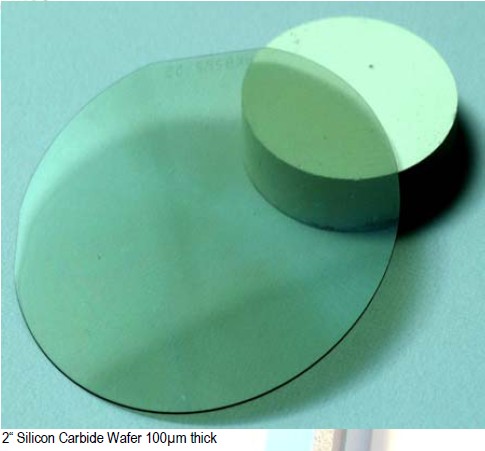
As the technology leader in the manufacture of vitrified super abrasives, Meister Abrasives has developed a new range of vitrified diamond super abrasives that enable fine grinding of very thin Silicon Carbide substrates down to 100μm or less.
Application
The objective of Silicon Carbide fine grinding is to avoid the costly lapping processes and reduce or eliminate the long CMP or polishing process time by using ultra fine diamond grit sizes in the grinding wheel.
The solution
Depending on wafer thinning requirements, Meister Abrasives offers various solutions:
• For rough grinding the use of Meister Abrasives VIT-DIA 325 / 550 or 800 Mesh is recommended.
• For fine grinding the use of Meister Abrasives VIT-DIA 5000 / 8500 Mesh is recommended.
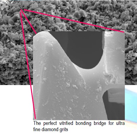
Vitrified diamond abrasive structure of ultra fine diamond grits sizes

Benefits of vitrified diamond bonding
The superior free cutting and self sharpening capabilities of the vitrified bonding technology allows consistent high precision stock removal at very low grinding forces. This results in lower sub surface damage, improved TTV, Warp and Bow values on the Silicon Carbide substrates.


