Researchers develop an extremely simple procedure to obtain nanosized graphenes
Post Date: 25 Jul 2014 Viewed: 373

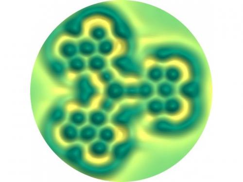
Atomic force microscopy (AFM) image of a clover-shaped nanographenes
The prestigious journal Angewandte Chemie has recently published a work by CiQUS researchers (University of Santiago de Compostela, Spain) in collaboration with IBM Research – Zurich (Switzerland), which describes an extremely simple method to obtain high quality nanographenes from easily available organic compounds. Graphene is considered an unique material, which is leading to the emergence of a completely new technology. One of the biggest challenges in this new field is the development of methodologies for the preparation on this material with nanometric size and high quality: if the researchers get a perfect control over their size and geometry, they could explore new applications for high-performance electronic devices. The method discovered by CiQUS researchers allows to obtain well-defined nanographenes in one-pot from perylene, a very common organic compound.
This method is based on the reactivity of a group of molecules named arynes, which can act as "molecular glue" to paste graphene fragments together. The clover-shaped nanographenes obtained in this research were deposited on ultrathin insulating films, and imaged with atomic resolutionby atomic force microscopy (AFM). The preparation of these materials with different size and shapes could be crucial to build graphene-based electronic circuits, molecular machinery and/or single molecule electronic devices.
The research work, led by Prof. Diego Pe�a, is a contribution of the research group COMMO, COMMO -belonging to CiQUS-, and includes the participation of Prof. Enrique Guiti�n, Prof. Dolores P�rez and the PhD student Sara Collazos. This COMMO group is pioneer on the synthesis of nanosized graphenes following bottom-up approaches through chemical methods in solution. The IBM Group (link is external) is specialist in the use of AFM with atomic resolution and in this work Dr. Leo Gross, Dr. Gerhard Meyer and PhD student Bruno Schuler were involved.
Both groups have already collaborated and published previous results in prestigious chemistry scientific journals as Science (2012), and currently they take part of the Large European Project PAMS (Planar Atomic and Molecular Scale Devices) (link is external), with a total budget over 9 million Euros. PAMS main objective is to developelectronic devices of nanometric-scale size, in order to get the extreme miniaturization of the equipment used in information technology and communication.�


